
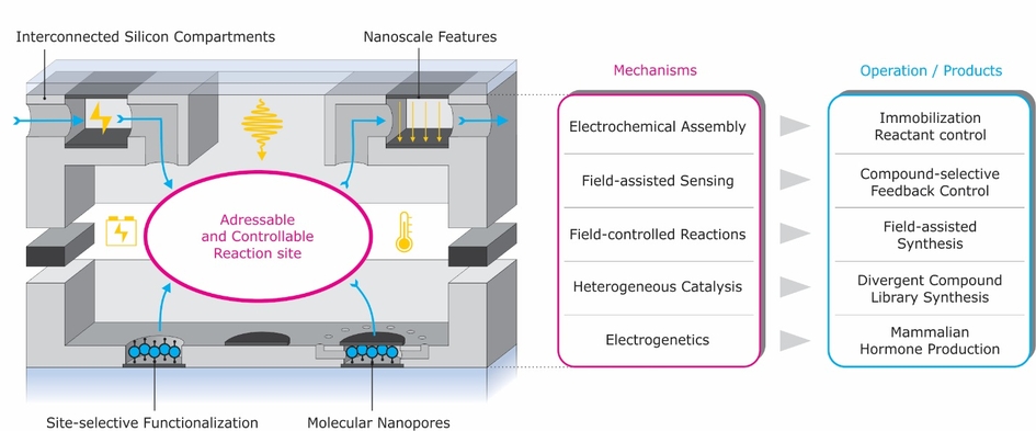
Constraining chemical reactions into physical compartments enables spatial control of reactants, stringent variation of reaction conditions and possibilities to locally apply electrical, electrochemical or optical stimuli. Such external “smart reagents” can reach high intensities and high gradients at nanoscale dimensions and allow thereby production rates to be regulated, reactivities to be switched on and off, selective reaction pathways to be chosen or even novel synthetic mechanisms to be introduced.
By top-down nanofabrication of scalable semiconductor devices with fluidic, electrical, electrochemical and optical access and site-selective functionalization by bottom-up molecular engineering, we can create molecular factories being able to produce added-value chemicals. Our solid-state compartmentalization approach leverages the high solvent compatibility and seamless sensing- and trigger-integration capability of silicon semiconductor platforms that we design, manufacture and package in-house in IBM’s Binnig and Rohrer Nanotechnology Center and IBM’s Noise-free Labs. Such silicon-based devices are used for a variety of tasks - ranging from fundamental science to applied research - in joint efforts within the NCCR MSE network:
joint research activity with Mayor group
 Interlinked Si-based reaction compartments with various exchange and communication paths. B) A nanoparticle adlayer acting as protective and electrical interfacial layer for subsequent metallization enabling molecular monolayers to be electrically contacted at two well-defined termini for energy-generation, sensing or storage and release of compounds used for synthetic operation and feed-back control thereof.") To reduce the complexity of multi-component reactions, individual reaction sites are physically separated into compartments, which are interlinked by microfluidics for mass-flow as well as electrical, optical and electrochemical exchange (Fig. 1A). Electrically contacted molecular monolayers (Fig. 1B) can exert molecular-intrinsic functionalities to be used for local sensing, energy-generation, storage or release sites (Fig. 1C).
To reduce the complexity of multi-component reactions, individual reaction sites are physically separated into compartments, which are interlinked by microfluidics for mass-flow as well as electrical, optical and electrochemical exchange (Fig. 1A). Electrically contacted molecular monolayers (Fig. 1B) can exert molecular-intrinsic functionalities to be used for local sensing, energy-generation, storage or release sites (Fig. 1C).
joint research activity with Mayor group
 can be released by applying an electrochemical bias to enable local click-chemistry build-up for a site-selective functionalization of enclosed compartments.") Electrode surfaces can be site-selectively functionalized by immobilizing a precursor compound with an electrochemically active protecting group that undergoes an irreversible chemical cleavage after reductive activation (Fig. 2A). This method allows chips with buried microfluidic channels and enclosed compartments to be efficiently functionalized by simple click-chemistry under mild conditions and with any desired functionalities (Fig. 2B).
Electrode surfaces can be site-selectively functionalized by immobilizing a precursor compound with an electrochemically active protecting group that undergoes an irreversible chemical cleavage after reductive activation (Fig. 2A). This method allows chips with buried microfluidic channels and enclosed compartments to be efficiently functionalized by simple click-chemistry under mild conditions and with any desired functionalities (Fig. 2B).
Optical Sensing of Molecular Binding Interactions
joint research activity with Mayor group
 Selective molecular binding between an immobilized receptor and an analyte change the dielectric environment of nano-structured surfaces (Fig. 3A). Their optical and electrical properties can be read-out by various modalities (Fig. 3B) leading to local sensing capabilities within a reaction compartment, a crucial requirement for feedback control in a molecular factory. For that task, we develop chemical anchoring concepts to adhere to both crystalline and amorphous silicon surfaces.
joint research activity with Mayor group
 or selectivity (C,D) among other functionalities.") Nanoscale separation of electrodes in semiconductor parallel-plate devices provides oriented electrical fields with amplitudes exceeding 109 V/m, giving rise to novel field-assisted chemistry. Combined with a directed assembly of molecular compounds on appropriated electrodes, such external fields can be used to control reactivity (Fig. 4A) or selectivity (Fig. 4B) in organic synthesis or to introduce novel synthetic processes.
Nanoscale separation of electrodes in semiconductor parallel-plate devices provides oriented electrical fields with amplitudes exceeding 109 V/m, giving rise to novel field-assisted chemistry. Combined with a directed assembly of molecular compounds on appropriated electrodes, such external fields can be used to control reactivity (Fig. 4A) or selectivity (Fig. 4B) in organic synthesis or to introduce novel synthetic processes.
joint research activity with Sparr and Mayor groups
 The site-selective functionalization of large arrays of reaction compartments on a silicon platform by catalytically active, immobilized compounds - in conjunction with local reaction control and nanoscale constraints - paves the way to synthesize large product libraries from a common starting material by combinatorial, divergent heterogeneous catalysis (Fig. 5). This effort finally aims at screening new synthetic pathways for drug discovery.
Apart from these activities, tailored silicon-based microfluidic hybrid devices, e.g. Silicon-on-insulator/glass devices with optical viewports and electrodes, are produced for oil-water and polymer-membrane soft-compartment generation, pico-injection and real-time sorting in a collaboration with the Panke, Pallivan and Meyer groups.
Additional funding is used in a close collaboration with the Fussenegger group on the development of an electrogenetic implant device that enables feedback control and telemetrical linkage to cognitive systems. See more details here.
Lörtscher group @IBM